
Week 4 Electronics production
Group assignment
- characterize the design rules for your in-house PCB production process
- send a PCB out to a board house
Individual assignment
Make and test a microcontroller development board
Group assignment
.jpg)
You can find the group assignment here
I’m entirely new to the concept of electronics so it was important to start from the basics
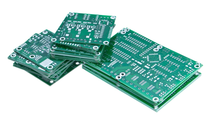
What is a PCB
A printed circuit board ( PCB ), also called printed wiring board ( PWB ), is a medium used to connect or "wire" components to one another in a circuit . It takes the form of a laminated sandwich structure of conductive and insulating layers: each of the conductive layers is designed with a pattern of traces, planes and other features (similar to wires on a flat surface) etched from one or more sheet layers of copper laminated onto and/or between sheet layers of a non-conductive substrate.
Types of PCB
Single-sided PCBs:
They represent the simplest form, featuring a sole layer of substrate with a thin conductive metal layer, commonly copper, etched to create the circuit pattern. Electronic components find placement on the opposite side of the board. These cost-effective PCBs find utility in straightforward electronic devices like power supplies, calculators, and radios.
Double-sided PCBs:
They elevate complexity by incorporating conductive metal layers on both sides of the substrate. Through-hole technology or surface mount technology facilitates connections between the two sides. This design flexibility is advantageous for intricate applications such as amplifiers, automotive dashboards, and HVAC systems.
Multi-layer PCBs:
They introduce a higher level of sophistication, consisting of multiple stacked layers with insulating material in between. Plated through holes connect these layers, allowing for 4 to 12 or more layers in high-density designs. Multi-layer PCBs are integral to intricate electronic systems like computers, satellites, and medical equipment.
There are two distinct ways to cut materials when CNC milling: Conventional Milling (Up) and Climb Milling (Down). The difference between these two techniques is the relationship of the rotation of the cutter to the direction of feed.
Making and testing a microcontroller development board
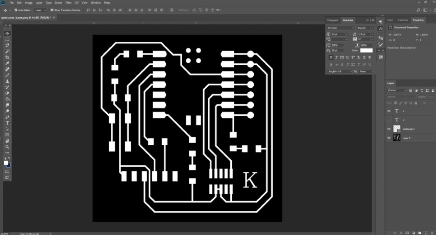
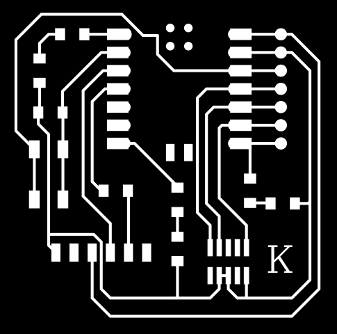
1.Personalising the trace
The design was provided in the fab academy. We downloaded the same and personalised it by adding our initials. I did the same in Photoshop.
2.Milling
Milling is the process of machining using rotary cutters to remove material by advancing a cutter into a workpiece . This may be done by varying directions on one or several axes, cutter head speed, and pressure.
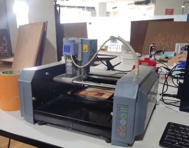
Roland Modela milling machine
The Roland Modela milling machine is a desktop-sized milling machine that is used for precision milling, drilling, and carving of a variety of materials such as plastic, wood, wax, and metal. It is manufactured by Roland DG Corporation, a Japanese manufacturer of digital fabrication tools and equipment
Fabmod
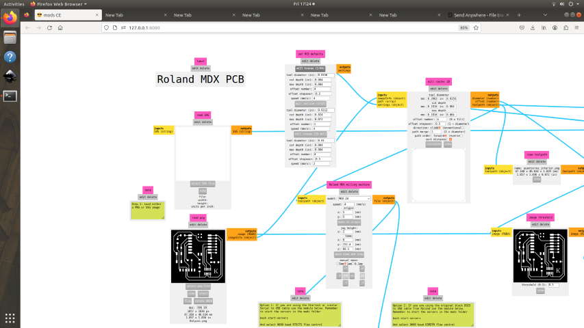
- The document was uploaded in PNG format.
- The origin was adjusted
- .4 mm bit was used for tracing and .8mm was used for cutting and drilling
- After adjusting the bit and sending the file the process took almost 30 minutes.
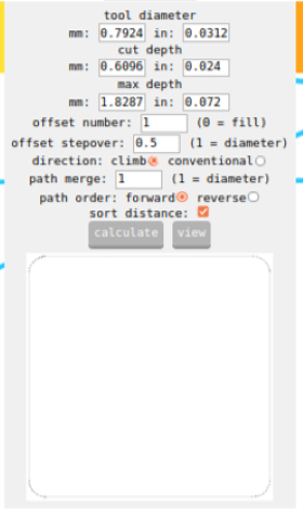
To cut the pcb the .8 bit is choosen and the tool path is calculated
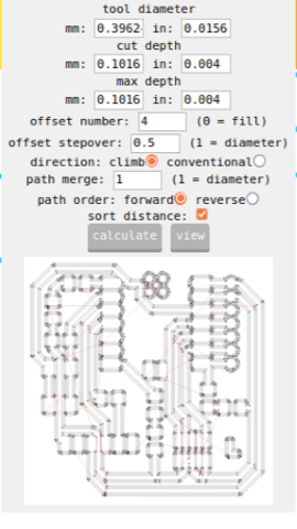
.4 mill is chosen for milling and the toolpath is calculated
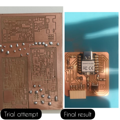
Milling Process
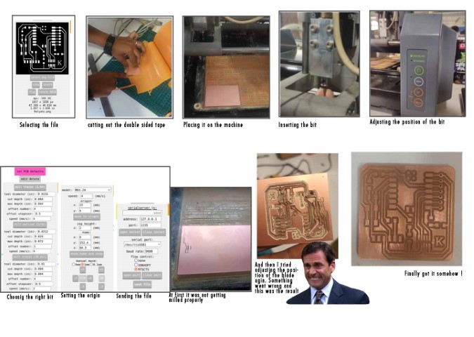
Mistakes made
- It’s important to be very careful while changing the bit or you might drop it and break it which I did
- Make sure to tighten the bit properly or you might get a hole in your PCB
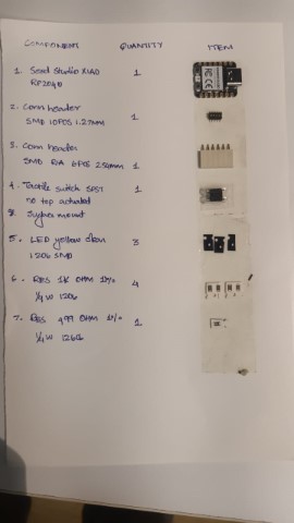
3.Collecting the components
Once milling was done we collected the components required from the material lab and made a list like this
4.Soldering
Soldering is a process used for joining metal parts to form a mechanical or electrical bond . It typically uses a low melting point metal alloy (solder) which is melted and applied to the metal parts to be joined and this bonds to the metal parts and forms a connection when the solder solidifies.
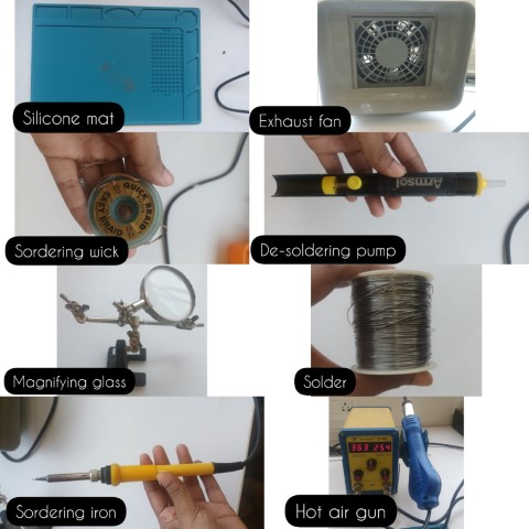
Soldering tools
Safety measures
-
Personal Protective Equipment (PPE):
- Wear safety glasses or goggles.
- Avoid loose clothing; opt for long sleeves and pants.
-
Work Area:
- Ensure good ventilation.
- Keep a fire extinguisher nearby.
-
Soldering Iron Safety:
- Set the iron to the right temperature.
- Use a holder; never touch the hot element.
-
Materials and Substances:
- Use flux in moderation.
- Wash hands after handling flux.
- Prefer lead-free solder.
-
Electrical Safety:
- Turn off and unplug the iron when not in use.
- Regularly check and replace damaged cords.
-
Workspace Organization:
- Keep the workspace clean and organized.
- Minimize distractions while soldering.
-
Training and Knowledge:
- Understand equipment and materials.
- Seek proper training if new to soldering.
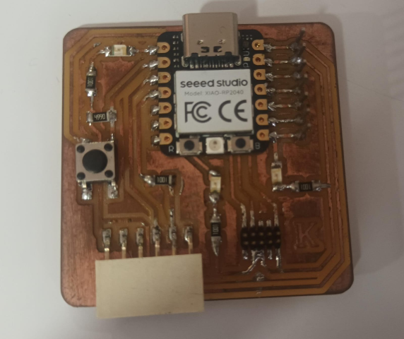
How I soldered
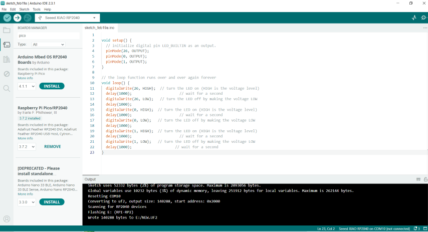
5.Programming
Quentorres
Quentorres board can program the new AVR Series 1 and 2 for example Adrianino and the ARMs for example SAMDino . It also has a button and an LED to learn to program in C, Rust, Go, Micropython... It has breakout pins in case you want to connect other external elements.
- Installed Arduino from here
- Followed the steps provided here
Open File > Preferences
.png)
Open Tools > Board > Board Manager . Type "pico" on the search bar and download Raspberry Pi Pico RP2040 .
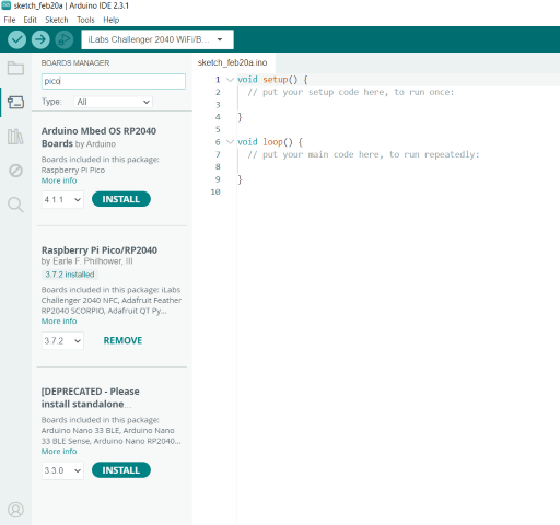
Once it is installed. Select Tools and follow the steps as given to select the board.
.png)
Then I modified the code to light the LEDs and uploaded to get the reults
Final result
Extras
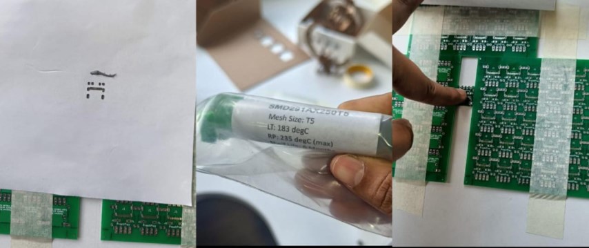
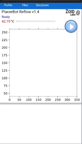
Reflow
As an extra assignment we did reflow soldering.
Reflow soldering
is a process in which a
solder paste
(a sticky mixture of powdered
solder
and
flux
) is used to temporarily attach one or thousands of tiny electrical components to their
contact pads
, after which the entire assembly is subjected to controlled heat. The solder paste reflows in a molten state, creating permanent solder joints. Heating may be accomplished by passing the assembly through a
reflow oven
, under an
infrared lamp
, or (mainly for prototyping) by soldering individual joints with a hot air pencil.
We made a stencil arrangement to perfectly fit the breakout board "ProshPlay" designed by Saheen Palayi in our lab.

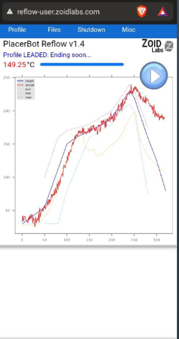
Preheat Phase: The PCB assembly is gradually heated to dry the paste and activate the flux, a chemical agent in the solder paste that cleans metal surfaces to improve the solder's ability to bond.
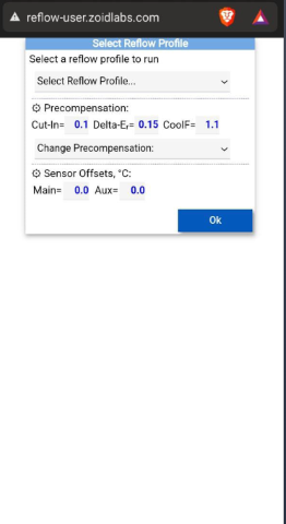
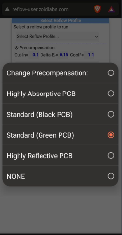
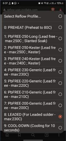
Done using an oven designed by a startup named "ZoidLabs
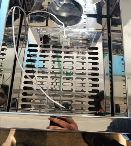
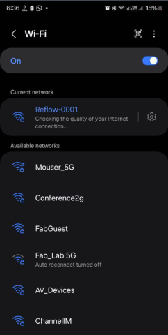
The following are the steps we followed to setup the oven
Files